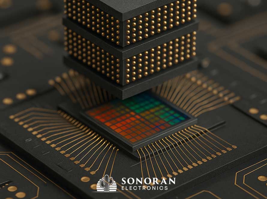
The semiconductor industry has spent decades making transistors smaller. Increasingly, however, engineers are exploring another way to increase computing density: building upward. Advanced packaging already allows separate semiconductor dies to be stacked and interconnected, while technologies such as high-bandwidth memory place multiple memory dies vertically within a single package. Monolithic three-dimensional integration takes this concept much further. Instead of manufacturing separate chips and stacking them later, engineers build additional layers of transistors directly above circuitry that has already been fabricated. The result could eventually be processors in which logic, memory, and specialized computing functions exist across multiple active semiconductor layers connected by extraordinarily short vertical interconnects.
Chip Stacking Is Already Here
Three-dimensional semiconductor systems are not new.
High-bandwidth memory stacks multiple memory dies vertically. Hybrid bonding allows semiconductor dies to be connected using extremely dense copper interconnects. Chiplet architectures combine multiple specialized dies within advanced packages. Three-dimensional NAND flash has demonstrated how vertical architectures can dramatically increase memory density.
But these approaches do not necessarily create a truly monolithic three-dimensional processor.
Most advanced packaging begins with semiconductor dies that have already been manufactured independently. Those dies are subsequently bonded together.
Monolithic 3D integration changes the sequence.
A transistor layer is fabricated, followed by another active transistor layer directly above it. Additional tiers can potentially be added afterward.
Instead of stacking completed chips, engineers are effectively building multiple floors of circuitry on the same semiconductor structure.
Why Vertical Distance Matters
The attraction is not simply fitting more transistors into the same footprint.
It is also about communication.
Modern processors spend enormous amounts of energy moving data between different parts of the chip and between processors and memory. As computing systems become larger, interconnects increasingly influence latency, bandwidth, and power consumption.
Monolithic 3D integration can dramatically shorten some of those connections.
Rather than routing a signal horizontally across a processor or through a package toward another die, a circuit could potentially communicate with another transistor layer directly above or below it.
The vertical distance might be extremely small.
This creates the possibility of extraordinarily dense interlayer connectivity—far denser than conventional package-level connections.
That characteristic makes monolithic 3D particularly interesting for artificial intelligence, where enormous amounts of data must continuously move between memory and computation.
Logic and Memory Could Become Neighbors
One of the most promising applications involves memory.
Traditional computing architectures physically separate processors and memory. Data must repeatedly travel between them, creating what engineers often call the memory wall.
High-bandwidth memory has significantly improved this relationship by placing memory much closer to AI processors. But HBM remains a separate semiconductor structure.
Monolithic integration could potentially bring certain types of memory even closer.
Imagine a processor with conventional high-performance logic on its bottom tier and memory circuitry fabricated directly above it. Instead of moving data across a circuit board or even across an interposer, information could travel vertically through extremely short connections.
More sophisticated architectures could incorporate additional layers dedicated to cache, memory, sensing, analog processing, or specialized AI computation.
The chip itself begins to resemble a vertically integrated computing system.
2026 Has Brought Important Demonstrations
This concept is moving beyond theoretical architecture.
Researchers reported in Nature in May 2026 that they had demonstrated wafer-scale monolithic integration using ultrathin single-crystal silicon membranes. The researchers sequentially fabricated as many as three transistor tiers while keeping processing temperatures at or below 400°C.
Importantly, the team did more than demonstrate individual transistors. They constructed vertically integrated logic gates, including inverters, NAND and NOR circuits, as well as SRAM cells.
The researchers also achieved inter-tier registration below 10 nanometers.
The work is important because one of the central challenges facing monolithic 3D has been creating upper-tier transistors with performance approaching conventional silicon devices.
If the transistors added to the upper floors of a chip perform significantly worse than those underneath them, much of the architectural advantage disappears.
The 2026 demonstration showed a potential pathway toward preserving silicon-class performance while building vertically.
Heat During Manufacturing Is a Major Obstacle
Ironically, one of monolithic 3D’s biggest thermal problems occurs before the processor is ever turned on.
Conventional transistor manufacturing often requires extremely high temperatures.
That is manageable when fabricating the first transistor layer. But once functioning transistors and metal interconnects already exist beneath the surface, manufacturing another layer at high temperature can damage them.
The industry therefore faces a strict thermal budget.
Upper transistor layers generally need to be manufactured at temperatures compatible with the completed circuitry below them.
This requirement is driving research into low-temperature semiconductor deposition, wafer transfer, oxide semiconductors, two-dimensional materials, and other manufacturing approaches.
A July 2026 Nature Communications study demonstrated complementary n-type and p-type transistor layers using indium oxide and tellurium deposited through low-temperature processes. The researchers fabricated CMOS inverters, multilayer logic, and a functional 3D SRAM cell while keeping processing below 300°C.
They also demonstrated a four-layer transistor stack.
That is an important distinction. Monolithic 3D becomes considerably more interesting when engineers can move beyond two active layers.
New Semiconductor Materials May Make 3D Easier
Silicon may remain the foundation of future processors, but upper transistor layers do not necessarily have to use exactly the same material.
Oxide semiconductors are particularly interesting because some can be deposited at relatively low temperatures.
Two-dimensional semiconductor materials are another possibility. Because these materials can form extraordinarily thin channels, they could eventually allow engineers to add transistor layers without consuming significant vertical space.
This opens the door to heterogeneous monolithic integration.
A future chip might use conventional silicon for its highest-performance logic while employing different semiconductor materials for memory, sensing, power management, or specialized computing layers above it.
The choice of semiconductor could become specific to each floor of the chip.
AI Could Be a Natural Application
Artificial intelligence hardware may provide one of the strongest incentives for developing these architectures.
AI workloads are unusually dependent on moving enormous quantities of data. Improving computational throughput alone provides diminishing returns if processors spend too much time and energy waiting for information.
Monolithic 3D provides another architectural tool for attacking that problem.
An August 2026 research demonstration used atomic-layer-deposited indium oxide devices to create three active tiers across 200 mm silicon wafers. More than 100,000 devices were fabricated, and researchers used the technology to develop a four-tier three-dimensional computing-in-memory accelerator aimed at large language model workloads.
The experimental architecture demonstrated performance improvements compared with corresponding two-dimensional implementations.
The significance is less about one specific accelerator and more about what the experiment demonstrates.
Monolithic 3D could allow designers to rethink where computation occurs.
Instead of continually moving information toward a centralized processor, portions of the computation could be distributed vertically throughout memory and logic layers.
Operating Temperature Creates Another Challenge
Solving the manufacturing thermal budget does not solve the thermal problem entirely.
A three-dimensional processor must also remove heat during operation.
In a conventional processor, heat-producing transistors sit relatively close to the chip surface, where thermal energy can eventually move toward a heat spreader and cooling system.
Stacking active transistor layers creates heat sources buried deeper inside the structure.
The middle layers are particularly problematic because heat may need to travel through other active semiconductor tiers before reaching an effective thermal path.
As more layers are added, thermal management can therefore become one of the fundamental limitations on monolithic 3D scaling.
This could require new materials, thermal vias, backside cooling, microfluidics, diamond heat spreaders, or entirely new approaches to processor thermal architecture.
Interestingly, this connects directly with another emerging semiconductor trend: advanced cooling can no longer be designed independently from transistor architecture.
Manufacturing Yield Becomes More Complicated
Yield presents another challenge.