For much of the past decade, industry attention focused on logic scaling, EUV lithography, and AI accelerators. In 2026, another narrative is gaining momentum: compound semiconductors are expanding across RF, photonics, and high-frequency applications, and the materials layer is becoming strategically significant.
Compound semiconductors such as gallium arsenide, indium phosphide, and gallium nitride offer electronic and optical properties that silicon cannot replicate efficiently. Higher electron mobility, direct bandgaps, and superior high-frequency performance make them indispensable in specific domains. As wireless bandwidth requirements grow and optical interconnects proliferate, these materials are moving from specialized niches into broader infrastructure roles.
RF front-end modules in 5G and emerging 6G development programs rely heavily on compound semiconductors. Power amplifiers, low-noise amplifiers, and high-frequency switches demand performance at frequencies where silicon struggles to maintain efficiency. As carrier aggregation and spectrum expansion continue, device complexity increases, and compound materials capture more design share within smartphones and base stations.
Data center architectures are also reshaping demand. Optical interconnects using indium phosphide and related materials are critical for high-speed transceivers that link AI clusters. As compute density increases, electrical interconnect limits push systems toward optical solutions. The performance of photonic components is directly tied to compound semiconductor material quality and yield.
Defense and aerospace applications add another layer of demand. Radar systems, satellite communications, and secure communication platforms often require high-frequency, radiation-tolerant devices. Compound semiconductors provide performance advantages in extreme environments where silicon-based solutions would require additional complexity or compromise.
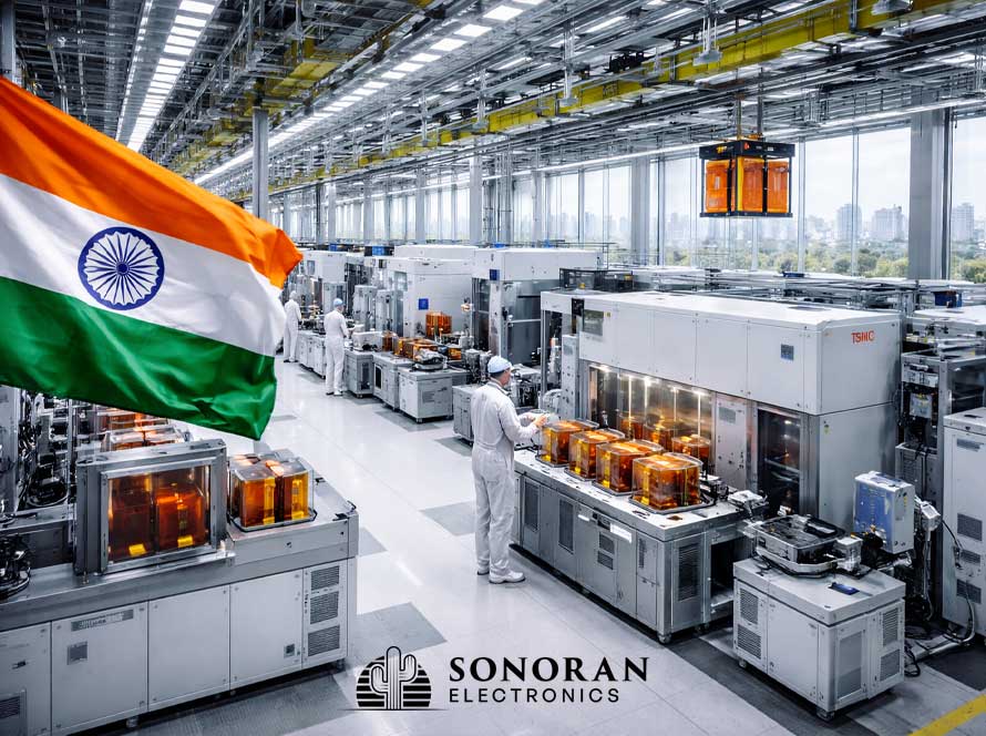
The supply chain is adapting unevenly. Wafer production for compound semiconductors remains more fragmented than silicon. Substrate scaling, defect reduction, and epitaxial growth consistency are ongoing technical challenges. Capital intensity is rising as manufacturers expand capacity to meet RF and photonics growth projections.
Pricing dynamics differ from silicon as well. Lower production volumes and specialized processing keep per-wafer costs elevated. However, value per die is often higher due to performance differentiation. In high-frequency and optical applications, device cost represents a smaller portion of overall system value, allowing compound semiconductor suppliers to maintain stronger pricing power.
Integration strategies are evolving. Some system designers pursue heterogeneous integration, combining silicon logic with compound semiconductor RF or photonic components within the same package. This approach leverages the strengths of each material while maintaining system-level compactness. Advanced packaging, therefore, becomes a convergence point between traditional silicon and compound materials.
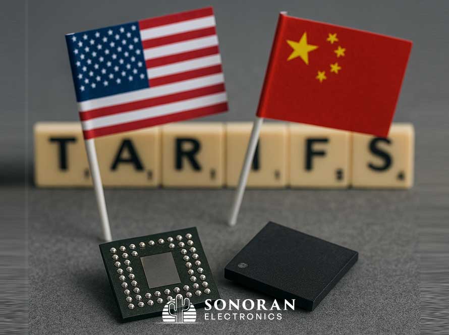
Geopolitical considerations intersect here as well. Certain compound semiconductor supply chains depend on critical minerals and specialized epitaxial processes concentrated in limited regions. As demand grows, governments are assessing supply resilience for both commercial telecommunications and defense systems.
The material layer has historically operated outside mainstream semiconductor discourse. In 2026, that distinction is narrowing. Performance gains in connectivity, photonics, and high-frequency systems increasingly depend on compound semiconductor advancement. The competitive edge is not only defined by transistor density, but by which materials enable the signals that move between them.