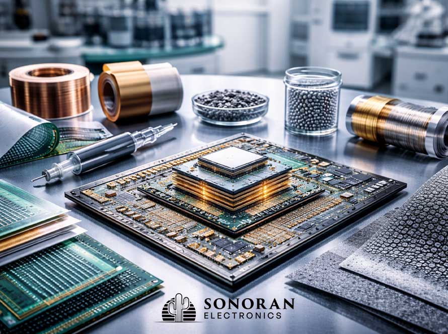
Modern microelectronics are marvels of precision engineering, containing billions of transistors packed into areas smaller than a fingernail. Yet few outside the semiconductor industry truly understand how these chips are made. Behind every integrated circuit (IC) lies a complex, multi-month process that transforms a raw silicon wafer into a highly specialized and densely packed microelectronic device. This article outlines the key steps in semiconductor fabrication, revealing the hidden science that underpins the digital age.
1. Silicon Wafer Preparation
The journey begins with high-purity monocrystalline silicon, derived from sand (silicon dioxide). Using the Czochralski process, a silicon seed crystal is dipped into molten silicon and slowly pulled upward, forming a cylindrical ingot. The ingot is then sliced into thin wafers—typically 200mm or 300mm in diameter—then polished to a mirror finish to ensure atomic-level smoothness. This substrate must be defect-free, as it will serve as the foundation for all subsequent microcomponent structures.
2. Photolithography
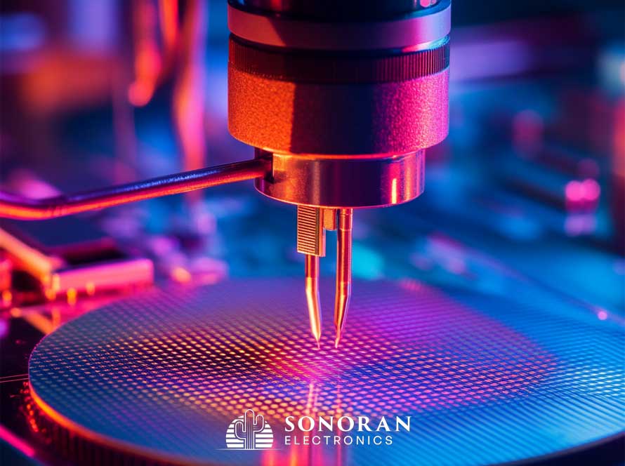
At the heart of chipmaking is photolithography, the process of transferring patterns onto the wafer using ultraviolet light. A layer of light-sensitive material called photoresist is spun onto the wafer surface. Then, using a photomask (a glass plate with transparent patterns), UV light is projected onto the wafer. The exposed photoresist is chemically altered and selectively removed, leaving behind a precise pattern that defines circuit elements such as gates, vias, or interconnects.
Extreme ultraviolet (EUV) lithography—now used at advanced nodes (7nm and below)—allows for smaller features by using light with wavelengths of just 13.5 nm. This technology is central to maintaining Moore’s Law.
3. Etching
Once the pattern is formed in the photoresist, etching removes the exposed material beneath it. There are two main types:
- Wet etching, which uses liquid chemicals for isotropic (uniform) removal.
- Dry etching, typically performed via reactive ion etching (RIE), which bombards the wafer with plasma for anisotropic, directional etching.
Etching creates the physical structure of transistor gates, trenches for interconnects, and vias between layers.
4. Doping (Ion Implantation)
To give regions of the silicon specific electrical properties, the wafer undergoes ion implantation. High-energy beams inject dopant atoms (like boron or phosphorus) into selected areas, altering conductivity. Doping is essential for forming p-type and n-type regions within transistors, enabling control of current flow.
Thermal annealing follows to activate dopants and repair crystal damage, typically using rapid thermal processing (RTP) techniques.
5. Deposition
To build up layers of material—conductors, insulators, or semiconductors—chemical vapor deposition (CVD) or physical vapor deposition (PVD) techniques are used. These layers include:
- Dielectrics (e.g., silicon dioxide or silicon nitride) to isolate layers.
- Conductors (e.g., copper or tungsten) to form interconnects.
- High-k dielectrics and metal gates in advanced nodes to reduce leakage.
6. Chemical Mechanical Planarization (CMP)
After multiple layers are deposited and patterned, CMP is used to flatten the wafer surface. This is critical for maintaining alignment between layers as complexity increases. A rotating pad and slurry containing abrasive particles polish the wafer to atomic-level uniformity.
7. Interconnect Formation
Modern chips contain dozens of metal layers that connect billions of transistors. These interconnects are formed by repeating cycles of deposition, lithography, etching, and CMP. Copper has largely replaced aluminum due to its lower resistivity and better scalability.
Low-k dielectric materials are used between interconnects to reduce capacitive coupling and improve signal speed.
8. Wafer Testing and Dicing
Once all layers are complete, the wafers undergo parametric testing and wafer-level burn-in to identify defective dies. The wafer is then diced into individual chips using laser or diamond saws. Each chip, or die, is inspected for mechanical integrity and electrical function.
9. Packaging and Final Test
Each die is mounted in a package that provides mechanical support and electrical connectivity to the outside world. Packaging technologies range from traditional lead frames to advanced 2.5D/3D integrated fan-out (InFO) systems. Wire bonding or flip-chip methods connect the die to the package substrate.
Final testing confirms functionality before shipment. Devices are often binned by performance, especially in CPUs or GPUs where slight variations affect speed and power consumption.
From start to finish, semiconductor fabrication involves over 1,000 individual steps, conducted in ultra-clean environments with nanometer precision. The entire process can take 12–16 weeks per wafer and involves contributions from materials science, physics, chemistry, and computer engineering. As the semiconductor industry pushes toward smaller nodes, more layers, and complex 3D integration, the science behind wafer-to-chip transformation continues to evolve.
For buyers and designers of microcomponents, understanding how chips are made helps explain why quality, consistency, and cleanliness are not just features—they’re prerequisites for performance.