2025 is shaping up to be a milestone year for quantum computing — and this has meaningful implications for the broader microelectronics industry, especially suppliers, packaging houses, and manufacturers who provide the foundational chips and substrates. Recent breakthroughs suggest that quantum‑classical integration is beginning to move from laboratory research into scalable manufacturing, creating demand for specialized microcomponents, cryogenic‑compatible materials, and hybrid architectures.
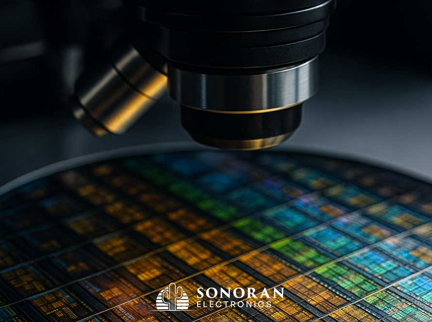
At the forefront of this shift are new quantum‑hardware developments: researchers at Princeton University recently unveiled a superconducting quantum chip whose qubits maintain coherence times more than three times longer than previously reported devices. Simultaneously, IBM announced progress toward fault‑tolerant quantum processors, scaling physical complexity by roughly an order of magnitude and transitioning towards 300 mm wafer fabrication — a technique shared with traditional semiconductor manufacturing.
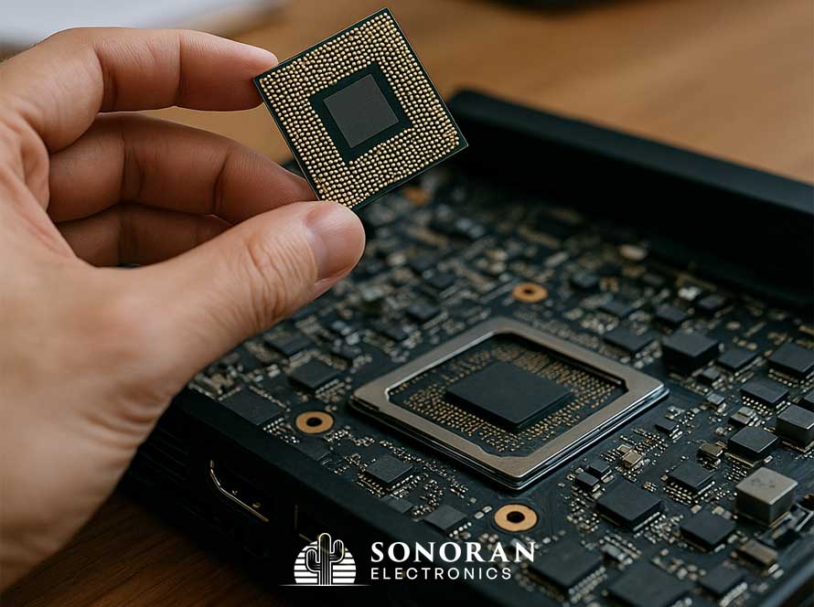
These developments matter because quantum chips are not isolated curiosities — they require entire ecosystems of materials, packaging, interconnects, thermal control, and classical‑to‑quantum interfaces (e.g. cryogenic control electronics, precision wiring, shielding). The manufacturing demands place pressure on microelectronics suppliers to deliver ultra‑clean substrates, precision interposers, and compliant components that operate reliably at cryogenic temperatures. For example, many quantum processors use superconducting circuits where even tiny impurities, dielectric losses, or thermal fluctuations can devastate coherence times. As a result, the standards for material purity, substrate quality, and packaging tolerances rise dramatically compared to conventional IC fabrication.
Furthermore, the trend toward hybrid quantum‑classical computing — where quantum processors are paired with high‑bandwidth classical accelerators (e.g. for data preprocessing, error correction, or post‑processing) — is driving demand for advanced heterogeneous integration. With quantum chips increasingly produced on similar wafer‑scale manufacturing flows, supply‑chain players may be called on to support mixed‑technology production: classical digital logic, analog, memory, RF, cryogenic control circuits, and quantum chips — all within a unified manufacturing and packaging workflow. This could accelerate adoption of modular packaging, chiplet architectures, and multi‑die integration practices previously popular with AI and HPC chips.
For suppliers and component distributors, these trends open both challenges and opportunities. On one hand, the tolerance thresholds and qualification requirements for quantum‑classical microcomponents will be tighter: greater purity, better thermal/cryogenic management, specialized packaging, and compliance with electromagnetic/noise isolation standards. On the other hand, serving the quantum‑classical market could become a high‑margin niche, especially for players who invest early in compatible materials (substrates, interposers, high‑reliability passives), specialized packaging, and testing services for cryogenic operation.
More broadly, the maturation of quantum hardware reminds the microelectronics industry that Moore’s Law and classical scaling are no longer the only frontier. Innovation is now branching into entirely different domains: quantum behavior, hybrid architectures, and cross‑domain integration. For suppliers and buyers of microcomponents, the message is clear: the definition of “microelectronics demand” is broadening — and those who adapt to include quantum‑classical systems may find themselves ahead in a landscape increasingly defined by versatility, precision, and high‑complexity integration.